ISP Pinout refers to a set of contact points on the mainboard of the Vivo Y29 4G, used for low-level Stock ROM flashing or recovery operations. These pins allow direct communication with the internal memory using specialized hardware tools such as UFI Box, JTAG, or other supported programming devices. By accessing these pins, technicians can perform tasks like unbricking, bypassing FRP, or flashing stock ROMs — all without removing the memory chip from the motherboard.
This interface is particularly useful when the device is bricked, stuck in bootloop, or not responding to regular flashing methods like Fastboot or emergency mode. Connecting through the ISP pinout allows direct access to the storage, making it an essential method for deep-level recovery.
Common Programming Interfaces and Pinouts
- USB – The most widely used interface. USB pinouts include VCC, GND, D+, and D−. It is standard for Stock ROM flashing and ADB/Fastboot operations.
- UART – A serial communication interface. Typical pins include RX (Receive), TX (Transmit), VCC, and GND. Often used in debug environments.
- JTAG – A professional interface for debugging and programming embedded devices. It provides full access to the microcontroller via multiple signal pins.
- SWD (Serial Wire Debug) – A simplified two-wire alternative to JTAG, used mostly on ARM-based microcontrollers for development and repair.
How to Use the ISP Pinout on Vivo Y29 4G
- Identify the correct ISP pinout points on the Vivo Y29 4G motherboard using a diagram or schematic.
- Use a supported flashing tool such as UFI, JTAG, or Easy JTAG to connect the pins to your PC.
- Carefully attach jumper wires or a test point adapter to the ISP pads.
- Launch your flashing software and proceed with reading or writing Stock ROM as required.
- Ensure a stable connection to avoid data corruption during the process.
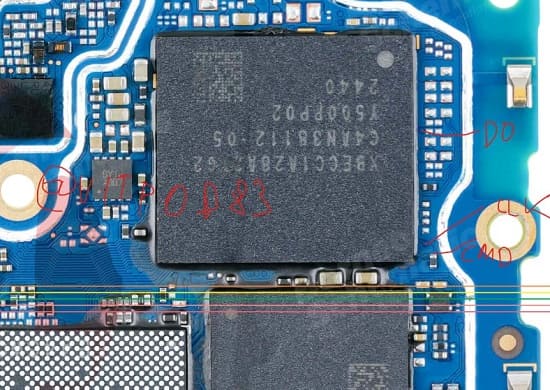
Vivo Y29 4G ISP Pinout Image